It is suitable for small portable devices.
Recently, the demand for smaller and thinner sized portable electronic communication devices, such as mobile and “Smart” phones, has increased significantly. As such, the electronic components used in these products need to be smaller and thinner to facilitate these more compact packages.
With that industry demand in mind, Seiko Instruments Inc. (abbr. “SII”, President: Masafumi Shimbo, Headquarter: 1-8 Nakase Mihama-ku Chiba-shi Chiba, Tel:+81-43-211-1111) will proudly introduce the world’s thinnest and smallest (1*) chip-type electric double layer capacitor, part number CP3225A, in October 2008.
The SII Electric Double-Layer Capacitor (EDLC) functions as a rechargeable electrical storage device, and is commonly used for mobile-phone memory and clock back-up during the primary battery’s run out or replacement.
Somewhat different than the coin cell battery that may often be used in these applications, this new device contains activated carbon, which has large surface area, in its electrode, while using organic solvent in the electrolyte.
Current EDLC packages are typically “coin” shaped, and don’t completely utilize the board space allocated to them due to the round shape. Also, metal solder tabs are always required for surface mounting, which increases size thickness.
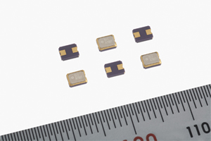
The new CP3225A product is “chip” shaped in an industry-standard rectangular package, effectively increasing volumetric efficiency by 50% (2*). In addition, by integrating tabs into the package itself, the CP3225A achieves a 20% reduction in mounting height – at only 0.9mm — the thinnest in the industry.
Ceramic has been chosen for the CP3225A’s package incorporating SII’s uniquely developed inner structure and encapsulating technique. This unique ceramic packaging offers superior air-tightness and leakage resistance compared to that of a coin-type package.
SII will continue to develop and expand the line-up of the Ceramic EDLC series.
(1*) the world’s thinnest and smallest -> as per SII research in Feb 2008
(2*) Compared with SII’s coin-type EDLC, XH 414HG-II02E
Main Characteristics
1.Chip-type/Smallest size: 3.2 x 2.5 x 0.9 mm
Compared with a standard coin-type EDLC (D: 4.8 H:1.7 mm), the new product realized a 1/5 reduction in mounting area. It is most suitable for smaller and thinner applications.
2.High capacity: 14mF
Compared with a similar sized tantalum capacitor, a chip-type EDLC contains over 30 times more electric capacity.
3.Max. charge voltage: 2.6V
Organic solvent in electrolyte allows for a wider voltage range, from 0 to 2.6V. Therefore, over-charge/over-discharge prevention circuitry is no longer necessary.
4.Quick charge characteristics
A 1 minute charge stores approximately 90% of full capacity. Also, with load current of 1-100uA, discharge capacity exceeds 90%. Furthermore, charge-discharge cycle is rated at more than 50,000.
5.Pb-Free Reflowable
Heat-resistant design allows for Pb-free reflowable SMT board attachment.
Application
Backup for memory, clock function and power management ICs for mobile-phones and most other portable electronic devices.
Sampling and Mass Production Schedule
Sample: Available from June 2008
Mass Production: Starts from October 2008
Sample Pricing
To be determined
